
TSV Cost Structure and Yield Ramp-Up in 3DIC
Through-silicon via, or TSV, technology sits at the heart of many advanced packaging and heterogeneous integration roadmaps. As the industry moves from 2D scaling to 3D integration, TSVs enable vertical stacking of dies, shorten interconnects, raise bandwidth, and improve system performance. Yet behind the impressive technical benefits lies a complex story of cost structure, yield ramp, and manufacturing learning curves that determine how quickly 3DIC can become mainstream in high-volume production.

Understanding the economics of TSV-based 3DIC means looking beyond simple wafer pricing. It requires a detailed view of process steps, materials, test strategies, die and stack yield, redundancy schemes, and integration choices across the entire production chain. As heterogeneous integration grows, this cost and yield picture becomes even more nuanced, because multiple technologies, nodes, and vendors come together inside one 3D stack. In this post, we explore how TSV cost structure is composed, how yield ramp-up works in practice, and what design and process strategies can make 3DIC economically viable in advanced packaging.
TSV and 3DIC in the Packaging Landscape
TSVs are vertical electrical connections that pass through the thickness of a silicon die, linking circuitry on the front of the wafer to another die or to the package substrate. In 3DIC, they are used to stack active dies, memory and logic, sensor layers, or RF and baseband components, enabling high-density, high-bandwidth interconnects. Compared to traditional wire bonding or long redistribution on a substrate, TSVs dramatically reduce interconnect length and parasitics, which translates into better performance and lower power for many applications.
From a packaging standpoint, TSV-based 3DIC is a natural evolution from 2.5D interposer-based solutions. Where 2.5D uses a silicon interposer with thousands of micro-bumps to connect side-by-side dies, TSV 3DIC takes the next step by stacking dies vertically. This yields even higher integration density and can shrink overall footprint, but it also introduces new process steps, new failure modes, and a more complex cost structure to manage.
Breaking Down TSV Cost Structure
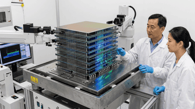
The cost structure of a TSV-based 3DIC can be roughly divided into four major categories: front-end TSV formation, back-end and thinning, stacking and bonding, and test and yield management. On top of these categories sits the overarching system cost impact, including design, packaging, logistics, and potential savings from heterogeneous integration choices.
Front-end TSV formation covers all steps needed to create the vias in the silicon wafer. This includes via etching, dielectric lining, barrier and seed deposition, and via filling, usually with copper or tungsten. These steps require specialized equipment and add extra process layers beyond a conventional front-end flow, directly impacting wafer cost. The via density and depth drive process complexity: higher aspect ratio TSVs and tighter pitches are costlier due to more stringent etch and fill requirements and tighter process controls.
Back-end and thinning add additional cost contributions. To expose TSVs for backside connection, wafers are thinned, often to tens of microns. This requires grinding, polishing, and temporary bonding to carrier wafers to maintain mechanical stability. Each step carries material and equipment costs, as well as yield risk: wafer breakage, warpage, and TSV exposure defects can all degrade effective yield and increase per-good-die cost.
Stacking and bonding include die attach, alignment, bonding of multiple wafer or die layers, and underfill or bonding materials. In 3DIC, stacking can be die-to-wafer, wafer-to-wafer, or die-to-die, each with its own tooling and cost profile. Precise alignment is critical to ensure TSVs and micro-bumps connect correctly; tighter tolerances mean more advanced, expensive bonders and longer cycle times.
Test and yield management costs often surprise newcomers to 3DIC economics. With multiple dies and TSV arrays in a stack, testing becomes more complex and must happen at multiple stages: wafer test for known good die, partial stack test, and final package test. Additional design-for-test logic, probing steps, and rework or scrap costs must be factored in. Tools like 3D cost modeling frameworks explicitly account for these contributions, showing how test strategy and yield assumptions significantly influence overall cost per functional stack.
Cost vs Performance: Why TSV Still Makes Sense
Given the extra process steps and complexity, TSV-based 3DIC clearly adds cost compared to a simple 2D device. However, for many advanced designs, the question is not whether TSVs are cheaper than traditional packaging, but whether they enable system-level cost savings or value that justify their incremental cost.
One key driver is the ability to partition a large, monolithic SoC into multiple smaller dies and stack them. Larger dies on cutting-edge nodes typically suffer from lower yields, driving up cost per functional die. By splitting the design into smaller logic dies plus a separate die for analog and I/O, the overall system can maintain performance while improving yield. In some cases, studies have shown that a heterogeneous 3D stack using advanced logic plus a cheaper, mature-node analog/I/O die can reduce total package cost by several percent compared to a scaled monolithic design, even when TSV and stacking costs are included.
Another driver is bandwidth and power efficiency. TSVs enable very wide, low-latency buses between stacked dies, such as in logic-plus-memory configurations. This can reduce the need for high-speed serial interfaces, simplify board design, and cut power consumption. For applications like high-performance computing or AI accelerators, these savings and performance gains can more than offset the higher packaging cost, especially when the system cost of the entire server or module is considered.
Yield: The Critical Lever in TSV Economics

Yield sits at the center of TSV cost structure. The yield of a 3DIC stack is the product of the yields of all its component dies and the yields of the stacking and TSV processes. If any die or TSV array is defective, the entire stack can be compromised. This multiplicative effect makes yield management and ramp-up especially critical for 3DIC projects.
At a simplified level, if each die layer in a three-die stack has a yield of 90 percent and the stacking process has 95 percent yield, the resulting stack yield is roughly 0.9 × 0.9 × 0.9 × 0.95, or about 69 percent, before considering TSV-specific failures. If the TSV process itself reduces effective die yield further, stack yield can quickly drop to uneconomic levels. This is why early 3DIC implementations often target high-value, low-volume applications where higher cost per unit can be tolerated.
However, yield is not static. As with any semiconductor process, it improves over time through learning, defect identification and reduction, and process control enhancements. Yield ramp-up for TSV-based 3DIC follows a curve where initial, small-volume production may be costly, but continuous tuning and monitoring can push yields upward toward levels that support broader volume deployment. The key is careful management of TSV failure mechanisms and robust process monitoring across all steps, from via formation to final package test.
TSV Failure Mechanisms and Their Cost Impact
To improve yield and control costs, manufacturers must understand where and how TSVs fail. Defects can arise during via etching and fill, such as voids, seams, or residues that compromise conductivity or reliability. Stress-related issues, including cracking or delamination around the via, can emerge during wafer thinning or thermal cycling. Bonding defects can misalign or leave interconnects open or shorted. Each failure mode can manifest as a latent reliability risk or as an immediate open/short, both of which reduce effective yield.
Every failed TSV that leads to a bad die or stack represents sunk cost: the wafer has already undergone expensive TSV formation and thinning, the die has been bonded and partially assembled, and test resources have been consumed. In aggregate, such losses can heavily skew the cost structure, particularly in early production where failure rates are higher. Understanding TSV failure statistics and targeting the most impactful failure modes yields outsized economic benefits during yield ramp-up.
Redundancy and TSV Grouping Strategies

One widely used approach to improving effective yield in 3DIC is redundancy at the TSV and interconnect level. Instead of relying on a one-to-one mapping between logical connections and TSVs, designers allocate spare TSVs and employ grouping schemes where multiple TSVs jointly support a set of signals. If one TSV in a group fails, the design can re-route signals through redundant paths or use multiplexers to avoid the defective via.
Careful TSV grouping and redundancy planning can dramatically increase yield without linearly increasing the number of TSVs and associated cost. Research has shown that choosing appropriate grouping ratios can achieve near 100 percent functional yield for a given TSV failure rate, with modest hardware overhead. The trade-off involves the extra area for redundant TSVs, routing complexity, and multiplexing logic versus the cost savings from higher effective yield and fewer scrapped stacks.
From a cost structure perspective, redundancy shifts some cost from variability and scrap into silicon area and design complexity. The net effect, when well-optimized, tends to be favorable, particularly for high-value 3DIC products where the cost of losing a partially assembled stack is substantial. Redundancy is thus a central tool in the economic optimization of TSV-based integration.
Known Good Die and Test Strategy
Another lever in yield and cost is the use of known good die, or KGD, and comprehensive test strategies. Because a single bad die can spoil an entire stack, testing dies before stacking is critical. Wafer-level tests aimed at verifying TSV integrity, functional performance, and parametrics are deployed to identify and discard defective dies early, before incurring the cost of stacking and packaging.
However, KGD testing introduces overhead: additional probes, test time, and design-for-test circuitry are needed. The cost impact depends on test coverage, test time per die, and the degree to which early removal of bad dies reduces downstream scrap. Effective test scheduling may involve multiple phases: initial wafer-level test to identify gross defects, partial stack test to verify inter-die connections, and final package test. Balancing the depth and timing of these tests is a complex cost-yield optimization problem, and sophisticated modeling tools are often used to explore trade-offs.
In heterogeneous 3D stacks, test complexity increases further because dies may come from different foundries or be manufactured on different process nodes with distinct defect signatures. Standardized test interfaces and design-for-test features become even more important to ensure consistent KGD approaches across the stack and to integrate multi-vendor dies efficiently.
Process Scaling, TSV Dimensions, and Learning Curves
TSV cost and yield are also influenced by TSV geometry and process scaling. Smaller-diameter TSVs with finer pitch enable more connections per unit area and support denser stacking, but they also push etch, fill, and alignment capabilities to their limits. This can initially raise defect rates, slowing yield ramp-up. Over time, as processes mature and equipment improves, the defectivity associated with finer TSVs can be reduced, enabling better cost-performance ratios.
Manufacturing learning curves play a significant role. Early adopters typically accept higher costs as they develop process recipes, tune equipment, and build data on defect modes. As experience accumulates, process windows expand, variability shrinks, and yield improves. This is how TSV 3DIC transitions from specialty technology to a more standard part of the advanced packaging toolbox. For design and business planning, it is crucial to anticipate this learning curve and recognize that cost models based on early pilot lines may overstate long-term production costs.
Heterogeneous Integration and System-Level Cost
Heterogeneous integration complicates TSV cost analysis but also amplifies its benefits. In a heterogeneous 3DIC, different dies can be optimized independently: analog and RF blocks can remain on mature nodes, digital logic can migrate to advanced nodes, and specialized accelerators or memory can be fabricated in processes best suited to their functions. TSVs tie these dies together into a compact, high-performance system.
System-level cost modeling that includes TSV stacking must consider more than per-wafer or per-package costs. It should account for yield differences between nodes, relative cost per square millimeter of silicon, design reuse, performance gains, and potential reductions in board-level complexity. In some realistic design scenarios, heterogeneous 3D stacking has been shown to reduce large-die system cost by several percentage points compared to pure scaling of a monolithic SoC, even after incorporating TSV and stacking costs. This underscores the importance of treating TSV 3DIC as a system design option rather than a simple packaging add-on.
Design and Integration Strategies for Better Economics
To make TSV-based 3DIC economically attractive, design teams need to co-optimize architecture, TSV usage, redundancy, and test strategies from the outset. Partitioning a system across dies should be done with yield and cost in mind: where can logic be split to minimize die area while preserving performance? Which interfaces demand high-density TSV connections, and which can use fewer, reliable connections with redundancy?
Reducing TSV count where possible lowers both cost and failure exposure. This can be achieved through architectural choices such as aggregating signals, using wide buses only where truly needed, and leveraging high-level protocols that minimize wire count. At the same time, for heavily used links such as memory channels, high TSV counts are unavoidable, making redundancy and robust test especially critical in those regions of the design.
Early collaboration between design, process, and packaging teams is essential. A package-aware design approach that considers mechanical stress, thermal paths, and TSV placement can mitigate failure risks, improve yield, and reduce rework. Likewise, process engineers can provide realistic TSV process capabilities and defect statistics, which inform redundancy and test planning in the design phase rather than after tape-out.
Ramp-Up Strategies and Risk Management
As companies move from prototype to volume production of TSV-based 3DICs, ramp-up strategies must balance risk and cost. One common approach is to start with smaller stacks or lower TSV densities, targeting applications that can tolerate higher cost but demand the performance benefits of 3D integration. This allows process learning and yield improvements to occur in a controlled environment.
Over time, as yields improve and cost per stack falls, designers can increase stack heights, TSV densities, and product mix. Parallel investments in equipment, metrology, and defect analysis capabilities accelerate this ramp-up. Using structured, data-driven yield learning programs and cost modeling tools helps management decide when to expand capacity, when to transition designs to finer TSV geometries, and how to prioritize product introductions.
Risk management also extends to supply chain considerations. TSV 3DIC often involves multiple partners, including wafer foundries, TSV processing facilities, OSATs, and test houses. Coordinating quality, logistics, and process integration across these entities is vital to ensuring that yield improvements in one part of the chain are not offset by new issues elsewhere.
Conclusion: TSV Economics as a Path to Scalable 3DIC
Through-silicon vias and 3DIC represent a powerful set of tools for advanced packaging and heterogeneous integration. They enable new architectures, higher performance, and more efficient use of silicon across process nodes. But their widespread adoption depends on mastering a complex cost structure and driving effective yield ramp-up across all stages of the process.
By breaking TSV cost into front-end formation, back-end thinning, stacking and bonding, and test and yield management, stakeholders can systematically identify where to focus improvement efforts. Redundancy schemes, known good die strategies, and thoughtful architectural partitioning all contribute to better economics. Over time, manufacturing learning curves and heterogeneous integration benefits can turn TSV 3DIC from a cost adder into a net cost saver at the system level.
As the industry continues to push beyond 2D scaling, those who understand and optimize TSV cost structure and yield ramp dynamics will be in the best position to leverage 3DIC as a foundational technology. Advanced packaging is no longer just the last step in the flow; with TSVs and heterogeneous integration, it has become a central arena where performance, cost, and innovation converge.





